AFM Nanolithography
NanoFrazor – Thermal Probe Nanolithography
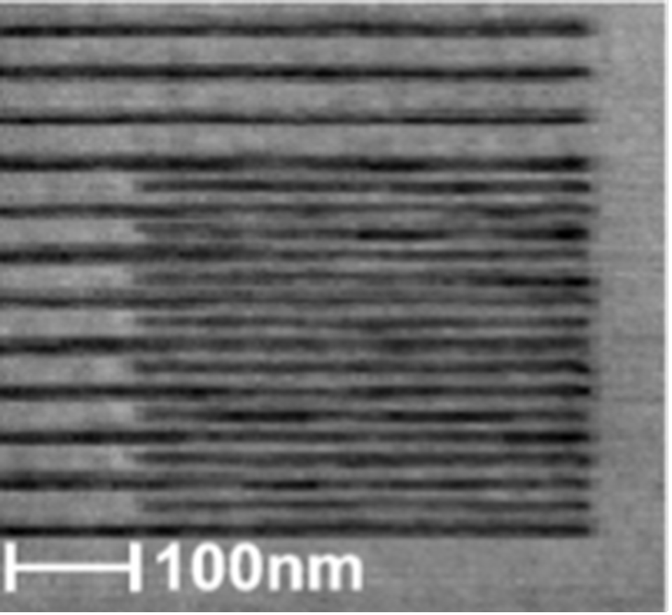
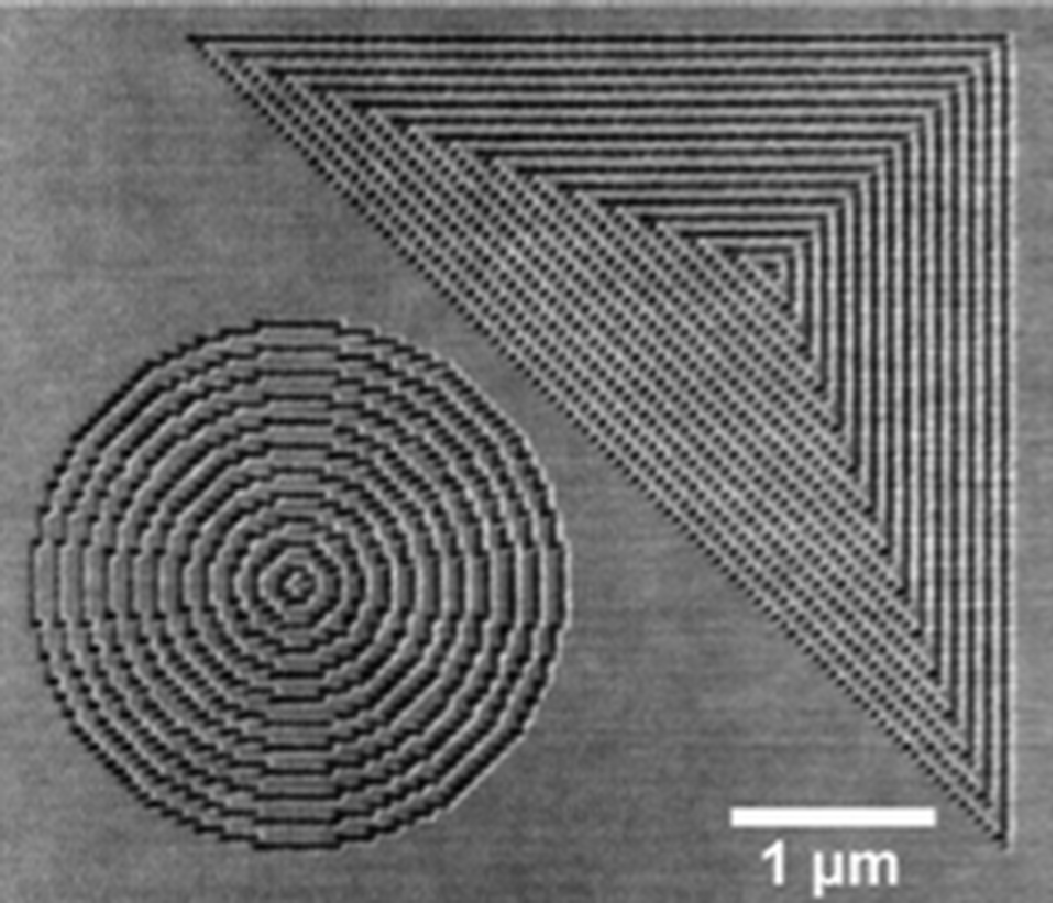
Heated tips offer the possibility to create arbitrary high-resolution nanostructures by local decomposition and evaporation of resist materials [1,2]. Closed-loop lithography and turnaround times of minutes are achieved with this patterning method due to the high-speed direct-write process and an in-situ imaging capability [3]. A marker-free stitching method [4], compatibility with CMOS processes [1,2,5] and high precision 3D patterning [1,2,5,6] complement this novel nanolithography concept. The technology has been developed at IBM and is now commercialized by SwissLitho, a spinoff company of the LSST.
![Enlarged view: Direct-write of 3D nanostructures: Topographical world map consisting of 5·10^5 pixels with a pitch of 20 nm written into PPA. The depth of the oceans is 80 nm, the patterning depth of the land corresponds to the respective altitude. [2]](/research/patterning/afm-nanolithography/_jcr_content/par/fullwidthimage_1522622624/image.imageformat.lightbox.603902682.png)
![Enlarged view: Field-stitching: Four fields stitched around a central pattern. The in-situ imaging capability and the natural surface roughness of the polymer were used for the stitching process. The Vernier dials in the corners of the fields reveal the achieved stitching accuracy of around 10 nm. [4]](/research/patterning/afm-nanolithography/_jcr_content/par/fullwidthimage_2090690418/image.imageformat.lightbox.1101975369.png)
![Enlarged view: Directed assembly and placement of nanoparticles: Shape matching traps have been fabricated in PPA and filled with gold nanorods using Capillary Assembly (a),(b). The PPA traps were removed by heat without disturbing the lateral position of the nanorods (red outline in b). A 10 nm off-axis positioning accuracy was achieved (c). [6]](/research/patterning/afm-nanolithography/_jcr_content/par/fullwidthimage_1037940466/image.imageformat.lightbox.54490209.png)
![Enlarged view: Archival data storage: 3-level data pattern written in PPA using the NanoFrazor and transferred into a stacked Si storage medium using RIE. The data is read with probe microscopy and the error rate is less than 10-3 (erros indicated in color). The inlet shows an optical microscopy image of the data pattern in the stacked Si storage medium. It shows a high optical contrast, which allows additional fast optical read-out. [5]](/research/patterning/afm-nanolithography/_jcr_content/par/fullwidthimage_1952733037/image.imageformat.lightbox.1316511832.png)
References
[1] Pires et al., Science, 328, 732, (2010).
[2] Knoll et al., Advanced Materials, 22, 3361, (2010).
[3] Paul et al., Nanotechnology, 22, 275306, (2011).
[4] Paul et al., Nanotechnology, 23, 385307, (2012).
[5] Holzner et al., Applied Physics Letters, 99, 023110, (2011).
[6] Holzner et al., Nano Letters, 11(9), 3957, (2011).
Funding
SNF project 126905: Surface structuring by means of stimulated desorption of organic material
Partners
SwissLitho AG external pagehttp://www.swisslitho.com
IBM Research Zurich external pagehttp://www.zurich.ibm.com
Contact
Felix Holzner