Flat Bimetallic Patterns
We developed a method to obtain bimetallic films in which two different metals form designed micro- or nano-patterns at the surface, and where the lateral interface between the two metals is characterized by topographic continuity, with the surface being overall ultraflat (roughness < 1 nm).
As a first step, a template is prepared by coating an ultraflat silicon wafer surface with a double layer of photoresist and by inscribing a certain design on it. This is done by means of photolithography for micrometric structures and e-beam lithography for nanometric structures.
Then, a first metal (gold or titanium) is evaporated on the template. After lift-off of the residual resist, a second metal (silver or gold) is evaporated on the wafer as a backfill.
A rigid support is either glued or welded to the metal and then mechanically stripped, in order to separate the bimetallic layer from the wafer. The revealed patterned metal surface is ultraflat as a result of having been formed in contact with the ultraflat silicon wafer.
![Enlarged view: Figure 1: Schematic of the procedure for obtaining ultraflat surfaces with bimetallic patterns [1].](/research/patterning/flat-bimetallic-patterns/_jcr_content/par/fullwidthimage/image.imageformat.lightbox.2058587236.png)
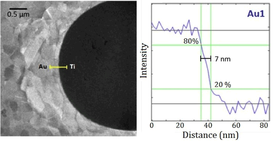
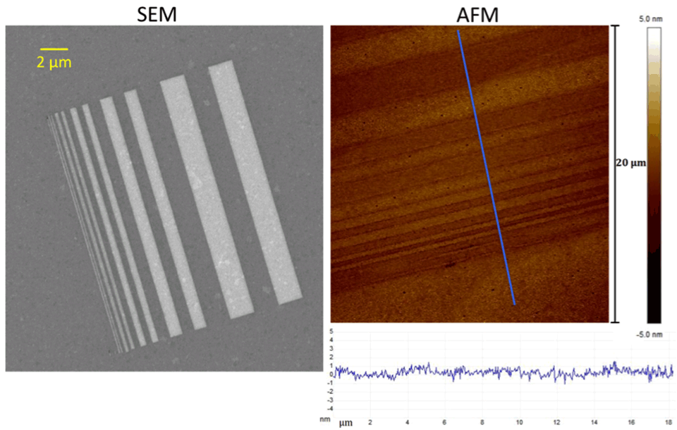
The low surface roughness and the topographical continuity at the interface of the two metals have been verified by atomic force microscopy (AFM).
X-ray photoelectron spectroscopy (XPS), time-of-flight secondary-ion mass spectrometry (ToF-SIMS) and Auger electron spectroscopy (AES) measurements have been carried out for the chemical characterization of the surfaces.
The results showed a sharp chemical contrast between the two metals at the lateral interface. This sharp contrast, in combination with the absence of topography, makes the samples suitable for application as calibration standards for the measurement of image and spectroscopic resolution of surface analysis instruments.
For the purpose of calibration, patterns have been specifically designed with different shapes and sizes for the measurement of resolution in each of the surface techniques considered (XPS, ToF-SIMS, AES).
References
1 N. V. Venkataraman, J.Pei., Clément V. M. Cremmel, A. Rossi and N. D. Spencer, Template-Stripped, Ultraflat Gold Surfaces with Coplanar, Embedded Titanium Micropatterns. Langmuir, 2013. 29.